| Sep 2024 Issue 24 | ||||||
 |
||||||
|
|
| Research | |
| Silicon Photonics – An Introduction | |
|
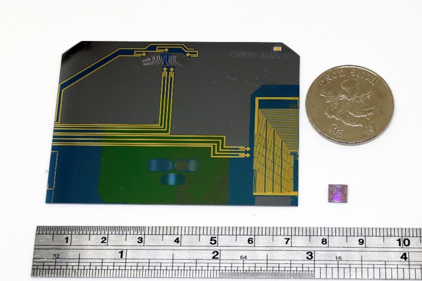
Author: Professor Hon Ki Tsang, FIEEE, Dean, Faculty of Engineering, WeiLun Professor of Electronic Engineering The billions of transistors within a silicon microelectronics chip are connected together by copper interconnects (photolithographically patterned fine lines of copper on the silicon chip), and each copper interconnect will dissipate a small amount of energy every time the voltage of the interconnect is switched. With billions of wires in the chip, the energy dissipation adds up to heat-up the whole chip, causing large increases in the chip temperature when the maximum possible switching frequency is exceeded. In 2004 researchers at Intel estimated that the heat generated per unit volume in a microprocessor could exceed that at the core of a nuclear reactor if all the wires were switched at the maximum operating frequency of the transistors, and the whole chip would melt! The individual silicon transistor can be switched can be as fast as five hundred billion times per second (500GHz), but the problem of heat dissipation in the copper interconnects within highly integrated computer processors has limited the switching frequency (the internal clock frequency of the microprocessor) of computer processors to only about 5 billion times per second (5GHz), more than 100 times slower than the potential maximum processing speed of the individual transistors. Computer clock frequencies have not significantly improved in the last 20 years because of this problem. Silicon photonics is a possible solution to this problem. Silicon photonics is based on the use of the same fabrication technology as has been perfected in the manufacture of previous generations of microelectronic integrated circuits, but instead of using copper wires and electrical signals for carrying data, silicon photonic integrated circuits use optical “wires” which guide light waves in tiny channels of silicon known as silicon optical waveguides. Fundamentally high-speed data transmission using light does not generate heat and hence optical interconnects can potentially make computers 100 times faster. Fig. 1 (a) Comparison of the cm scale silicon photonic chip which implemented an arrayed waveguide grating optical spectrometer with 40 wavelength channels made by Bookham Technology in 2002 (left) with the latest generation silicon photonics chip designed by Prof Tsang’s team manufactured in 2023 (lower right). The 1 dollar coin is for size comparison. Advances in silicon photonics in the last 20 years has led to about one million times reduction in chip area for the same spectrometer functionality.
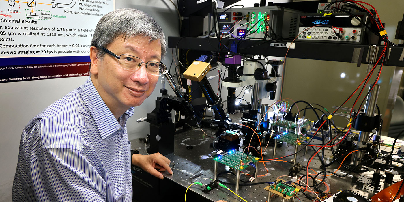
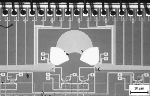
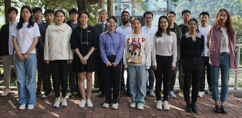
The silicon optical waveguides are based on the same physical principles as optical fibers, with the light confined at the waveguide walls by the phenomenon of total internal reflection made possible by silicon having a higher refractive index than its surrounding material (typically silicon oxide or air). Silicon has a refractive index of about 3.5, which is much higher than that of glass (1.5) and hence the silicon optical waveguides are about 20 times smaller than the diameter of the core of the glass optical fibers used in optical fiber communications. My research team at CUHK has been working in the field of silicon photonics for about 25 years: Two decades ago silicon optical waveguides were limited to relatively large sized shallow etched rib waveguides which typically had waveguide widths of several micrometers , and minimum bend radii of a few millimeters resulting in quite large cm scale chips (Fig. 1) for use in optical fiber telecommunication systems for separating the different wavelengths of light in wavelength division multiplexed optical fiber communications. But with the development of higher resolution photolithography it is now possible to manufacture much smaller high index contrast waveguides with minimum bend radii as small as 3mm using 500nm width waveguides (easily with the capability of the deep ultraviolet photolithography systems widely used in silicon microelectronics more than a decade ago), and the development of the foundry business model for silicon photonics, the area occupied by silicon photonic integrated circuits have be reduced by about a million times (Fig.1), enabling more functional elements to be integrated in the silicon photonics chips to address different applications. At the Chinese University of Hong Kong my team (Fig. 2) of PhD students and postdoctoral fellows are exploring both the immediate practical applications of silicon photonics as well as more advanced and longer term potential applications. We have developed silicon optical modulators, which convert high speed electrical signals to optical signals, and transmit data at over 100Gbaud (100 billion symbols per second), and we have demonstrated over 400Gb/s data transmission using a single wavelength of light. We have developed optical signal processors which perform high speed unitary matrix operations. These devices will be a key enabling technology for future data center optical interconnects supporting the 3.2Tb/s data transmission soon to be needed with the continued growth of the internet and the rise in demand for artificial intelligence and training of large language models. Fig. 2 Prof. Hon Ki Tsang (8th from the left) and his research team.
|
|
 |
|
|
|
|||||||||||||||||||||||