|
Prof. CHEN Shih-Chi, Department of Mechanical and Automation Engineering Two-photon excitation (TPE) microscopy has been widely used in biological studies and scientific research since its introduction in 1990. Its capability of generating optical cross-sections in deep tissues at video rates or higher speeds has for decades solved many mysteries for biologists. However, some of the new applications, e.g. in vivo brain imaging on mice, call for more capable TPE microscopes with functions such as random-access imaging, programmable imaging plane, high-speed axial scanner for volume imaging, and higher imaging speed at tens of kilohertz. A typical 3D random-access microscope employs four acousto-optic deflectors (AODs) to arbitrarily access any point within the work volume at 10s - 100 kHz speed. Due to the superior speed, a random-access microscope can maximize the scanning time at selected regions, resulting in better signal-to-noise ratios at much higher frame rates than raster scanning systems. Although the AOD-based scanning methods are fast (10s kHz), the resolution is usually compromised as the focal point scans away from the original focal plane; in addition, the large longitudinal size of the point spread function (PSF) (~3-10 µm) makes it unsuitable for volumetric scanning. A variety of methods have been developed to overcome these issues, e.g. separation of lateral and axial scanning paths to minimize interferences among AODs, and application of high-bandwidth custom-built AODs in combination with high-performance control systems. These systems are complex and expensive, and require the four AODs to be synchronized; additional prism pairs are often required to compensate for the severe temporal dispersion from the AODs, making them difficult to use or maintain. A compact, low-cost, and versatile random-access imaging system that has comparable resolution to raster-scanning systems has yet to be developed.
Recently, Prof. Chen Shih-Chi's team in the Department of Mechanical and Automation Engineering has developed a new ultrafast random-access scanning method for TPE microscopy based on a digital micromirror device (DMD), achieving a scanning rate of 22.7 kHz, scanning range of 200 µm, and scanning resolution, i.e. minimum step size, of ~270 nm, in which the rate, range and resolution are only limited by the DMD. The DMD-scanner is inspired by the DMD-based ultrafast beam shaper reported recently by Prof. Chen's team, achieving simultaneous axial and lateral scanning via superposing and rapidly modulating designed binary holograms on the DMD, as illustrated in Figure 1. As every hologram corresponds to a specific point in space, the DMD scanner can move the focal point to any random location within its work volume range at equal speed, thereby realizing random-access imaging. Figure 2 shows the optical configuration of this compact TPE microscope based on a single DMD.
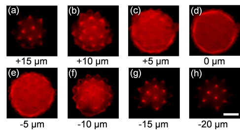
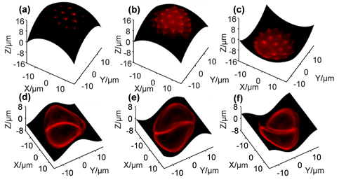
To measure the performance of the DMD-scanner, Prof. Chen's team performed imaging experiments on pollen grain samples with a 40x objective lens to examine whether the resolution would be negatively affected by the DMD-scanner. In the first experiment, the DMD was programmed to perform raster scanning, where the volume image of a single pollen, sized ~30 × 30 × 40 μm3, was obtained. The scanning was performed at 22.7 kHz, and the entire volume imaging process was completed within 3.6 seconds. Figures 3(a) – 3(h) present the results of 8 cross-sectional layers of the pollen, where individual spikes on the grain can be clearly visualized. Each layer has 100 × 100 pixels and is 5 μm apart; the brightness of each layer is normalized by its maximum fluorescence intensity. From the results, one can conclude that the imaging resolution and optical cross-sectioning capability of the scanless system is comparable to that of the conventional laser scanning TPE microscopes. The capability of scanning arbitrary paths in space means that the imaging plane can be arbitrarily programmed. This means it is feasible to programme the image plane to follow certain neuronal network in the brain, performing high-speed imaging experiments. Such a task cannot be achieved by conventional raster scanning systems. To demonstrate the capability, we scanned two different pollen grains on spherical and sinusoidal surfaces. The results are presented in Figure 4 (see Visualization 1 for video demonstrations). For the spherical surface, the scanning parameters should satisfy the surface function, i.e. (z1-z0)2 + x12 + y12 = R2, where z0 and R are constants; x1, y1 and z1 are proportional to fx, fy and 1/f, respectively. The sinusoidal surface profile was obtained via a similar procedure. The scanning was performed at 22.7 kHz, resulting in a frame rate of ~2.3 fps.
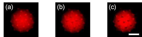
In the last experiment, we demonstrated 3D resolved random-access optical stimulation which can be realized by simply extending the dwell time of the laser focus at any selected point in space. For example, a dwell time of 1 millisecond allows 80,000 laser pulses to impinge the specimen, providing sufficient power and speed to stimulate, blaze, or even cut individual cells or tissues. Figures 5(a) – 5(c) present the selective optical stimulation results, where the seven selected spikes on the pollen volume image (Figure 3) are exposed to laser pulses for periods of 0, 3, and 15 seconds respectively at a low power level, i.e. 30 mW. From the results, one can clearly observe the effect of photobleaching, where the spikes no longer emit fluorescence signals and the adjacent areas remain unaffected.
In summary, experiments have been conducted to confirm that the DMD-scanner can perform XYZ scanning with comparable imaging resolution versus mechanical scanning. In addition, the TPE microscope based on this DMD-scanner can scan overly arbitrarily defined surfaces (i.e. spherical and sinusoidal surfaces) and perform ultrafast random-access imaging and stimulation. More importantly, many existing optical methods can be simultaneously implemented on the scanless TPE microscope via a single DMD, e.g. wavefront correction or compressive sensing, by superposing new hologram programmes of different purposes to scanning holograms. With versatility and high scanning rate, the new scanless TPE microscope may generate a significant impact on the field of biomedical imaging. In the near future, Prof. Chen's team will explore the combination of various beam modes, e.g. Bessel beam, to further enhance the performance of the TPE microscopy. The new TPE microscope system may find important uses in many emerging applications, e.g. high-speed in vivo imaging on the brain and bone marrow cavities.
|
|
|
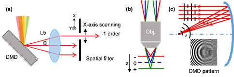
Figure 1. Working principles of the DMD-scanner: (a) lateral scanning on the focal plane, where x-axis scanning is realized via varying the spatial frequency fx. θ is the diffraction angle between the 0th and -1st order diffraction; (b) and (c) axial scanning along the optical path, where the holograms of spherical wavefronts are programmed to the DMD scanner; accordingly, the DMD functions as a concave/convex mirror with a positive/negative focal length.
|
|
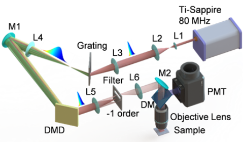
Figure 2. Optical configuration of the scanless TPE microscope based on a single DMD; M1, M2: high-reflectivity mirrors; L1-L6: lenses; DM: dichroic mirror; and PMT: photomultiplier tube.
|
|
Figure 3. Cross-sectional images of a pollen grain at eight different depths, scanned by DMD; the scale bar is 10 µm.
|
|
Figure 4. Cross-sectional images of two selected pollen grains on arbitrarily programmed spherical surfaces (a) - (c) and sinusoidal surfaces (d) - (f).
|
|
Figure 5. Photobleaching process of the seven selected spikes on the pollen grain for a total of (a) 0 second; (b) 3 seconds; and (c) 15 seconds; the scale bar is 10 µm.
|
|
|